Type A Type B Type C Type D Type E Type F Rayleigh Line
Pulse Forming Networks (PFNs) are used to generate output pulses which approximate a square wave shape. In their simplest form (e.g. Rayleigh lines), the use of an array of equal inductors and capacitors are used to approximate a transmission line with discrete elements. In other forms, the component values are optimized to synthesize a pulse output with minimum flattop ripple. In the examples below, 5 section PFNs are shown. Pulse Forming Networks with fewer sections can also be designed although they would typically generate more pulse ripple and longer pulse risetimes/falltimes. Conversely, more PFN sections can be designed to reduce the pulse ripple and the rise/fall times of the output pulse. Since PFNs approximate a transmission line, they must be charged up to twice the desired output pulse voltage since half the voltage is dropped across the PFN impedance and the remainder across the load impedance.
Examples of PFN systems designed by Ness Engineering staff can be found here on this webpage of Line Type Modulator Experience.
Each of the following waveform plots can be clicked on to open up the full size graph in a separate window.
Significantly more detail on PFN synthesis and design can be found in Chapter 6 of the book Pulse Generators by G.N. Glasoe and J.V. Lebacqz, published by McGraw Hill, New York in 1948.
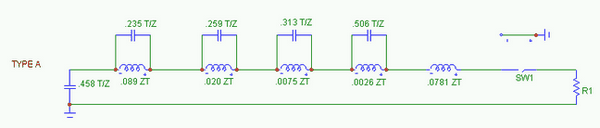
The circuit schematic for the Type A Pulse Forming Network is shown below. Type A PFNs are sometimes used with high voltage Marx banks acting as the primary capacitance (the capacitor on the far left of the schematic). The primary capacitance is initially charged and all other capacitances are uncharged. In this specific model, the primary capacitor has an initial condition voltage of 1000 V. For our example simulation, we have selected a pulse width (T) of 10 ms and a load impedance (Z) of 100 ohm. A switch is closed at approximately time 0 and the Pulse Forming Network discharges into the 100 ohm load impedance (resistor).
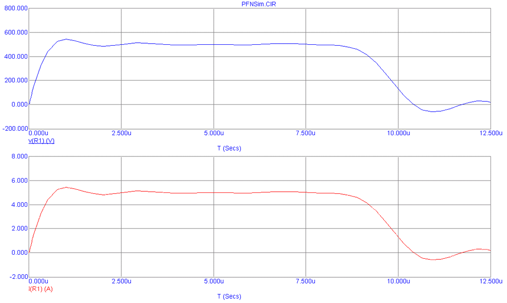
The results of the circuit model are shown below. V(R1) is the voltage across the 100 ohm load resistor. The circuit current, I(R1), is graphed in the second, lower plot. As noted above, the 1000 V initial condition results in a 500 V, 5 A square pulse into the 100 ohm load.
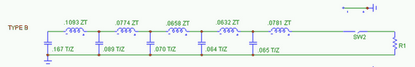
The circuit schematic for the Type B Pulse Forming Network is shown below. In this Type B PFN, each capacitance has an initial condition voltage of 1000 V. For our example simulation, we have selected a pulse width (T) of 10 ms and a load impedance (Z) of 100 ohm. A switch is closed at approximately time 0 and the Pulse Forming Network discharges into the 100 ohm load impedance (resistor).
The results of the circuit model are shown below. V(R1) is the voltage across the 100 ohm load resistor. The circuit current, I(R1), is graphed in the second, lower plot. As noted above, the 1000 V initial condition results in a 500 V, 5 A square pulse into the 100 ohm load.

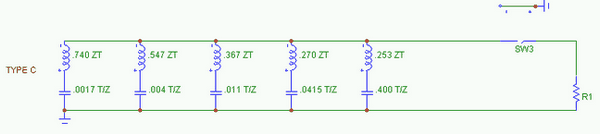
The circuit schematic for the Type C Pulse Forming Network is shown below. In this Type C PFN, each capacitance has an initial condition voltage of 1000 V. For our example simulation, we have selected a pulse width (T) of 10 ms and a load impedance (Z) of 100 ohm. A switch is closed at approximately time 0 and the Pulse Forming Network discharges into the 100 ohm load impedance (resistor).
The results of the circuit model are shown below. V(R1) is the voltage across the 100 ohm load resistor. The circuit current, I(R1), is graphed in the second, lower plot. As noted above, the 1000 V initial condition results in a 500 V, 5 A square pulse into the 100 ohm load.
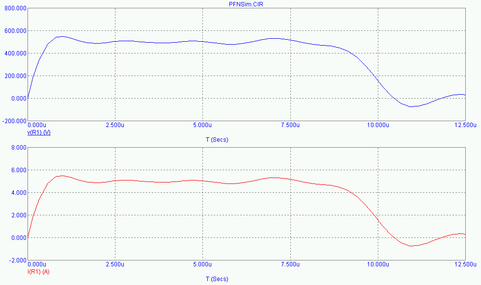
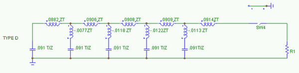
The circuit schematic for the Type D Pulse Forming Network is shown below. One advantage of the Type D PFN is that each section capacitance is equal, making the design and procurement simpler. However, although the Type D PFN is mathematically possible, realistic implementation is not because of the negative inductance values in series with each capacitor which are not physically realizable. For discussion purposes, we will still examine this case. In this Type D PFN, each capacitance has an initial condition voltage of 1000 V. For our example simulation, we have selected a pulse width (T) of 10 ms and a load impedance (Z) of 100 ohm. A switch is closed at approximately time 0 and the Pulse Forming Network discharges into the 100 ohm load impedance (resistor).
The results of the circuit model are shown below. V(R1) is the voltage across the 100 ohm load resistor. The circuit current, I(R1), is graphed in the second, lower plot. As noted above, the 1000 V initial condition results in a 500 V, 5 A square pulse into the 100 ohm load.
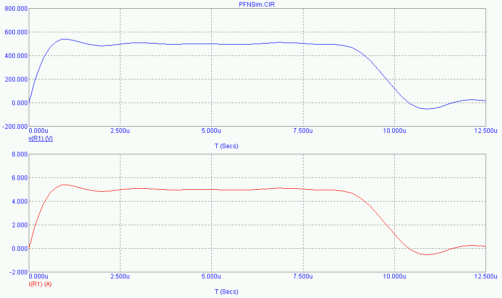
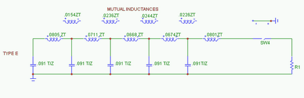
The circuit schematic for the Type E Pulse Forming Network is shown below. Type E PFNs are based upon the Type D PFN model but have been modified to allow realizable construction. The negative series inductances have been replaced with a set of mutual inductance values, making the algebraic sum of the inductances around each mesh the same in both the Type D and Type E designs. In many cases, coils can be wound on a single tubular form and their spacing adjusted in order to adjust the mutual coupling. In this specific model, each capacitor has an initial condition voltage of 1000 V. For our example simulation, we have selected a pulse width (T) of 10 ms and a load impedance (Z) of 100 ohm. A switch is closed at approximately time 0 and the Pulse Forming Network discharges into the 100 ohm load impedance (resistor).
The results of the circuit model are shown below. V(R1) is the voltage across the 100 ohm load resistor. The circuit current, I(R1), is graphed in the second, lower plot. As noted above, the 1000 V initial condition results in a 500 V, 5 A square pulse into the 100 ohm load.
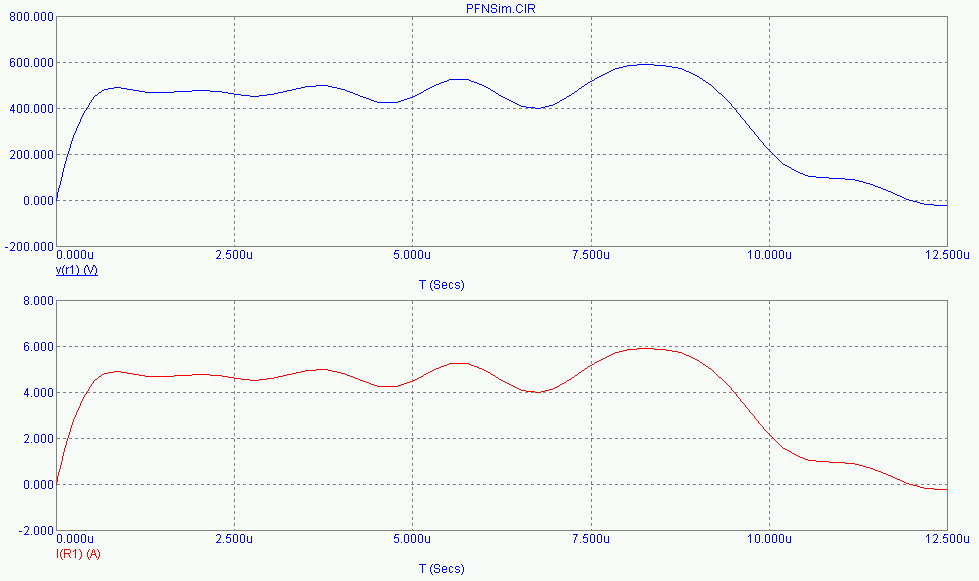
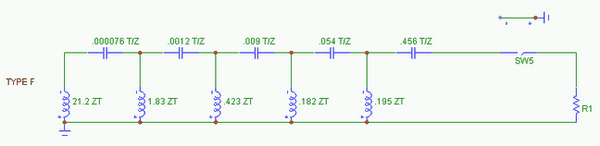
The circuit schematic for the Type F Pulse Forming Network is shown below. With the Type F PFN, the primary capacitance is the capacitor on the far right of the schematic (in this case, the 0.456T/Z value) and is initially charged up while all other capacitors are uncharged. In this specific model, the primary capacitor has an initial condition voltage of 1000 V. For our example simulation, we have selected a pulse width (T) of 10 ms and a load impedance (Z) of 100 ohm. A switch is closed at approximately time 0 and the Pulse Forming Network discharges into the 100 ohm load impedance (resistor).
The results of the circuit model are shown below. V(R1) is the voltage across the 100 ohm load resistor. The circuit current, I(R1), is graphed in the second, lower plot. As noted above, the 1000 V initial condition results in a 500 V, 5 A square pulse into the 100 ohm load.

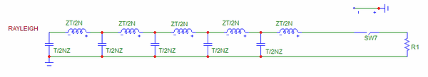
The circuit schematic for the Rayleigh Line Pulse Forming Network is shown below. Rayleigh Line PFNs are often used since they approximate a discrete element transmission line. The circuit capacitors and inductors are all equal values. Capacitor values are equal to the pulse duration divided by the product of two times the line impedance and the number of PFN sections. The inductor values are equal to the product of the pulse duration and impedance divided by the number of sections times two. Each capacitor has an initial condition voltage of 1000 V. For our example simulation, we have selected a pulse width (T) of 10 ms and a load impedance (Z) of 100 ohm. A switch is closed at approximately time 0 and the Pulse Forming Network discharges into the 100 ohm load impedance (resistor).
The results of the circuit model are shown below. V(R1) is the voltage across the 100 ohm load resistor. The circuit current, I(R1), is graphed in the second, lower plot. As noted above, the 1000 V initial condition results in a 500 V, 5 A square pulse into the 100 ohm load.

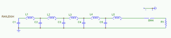
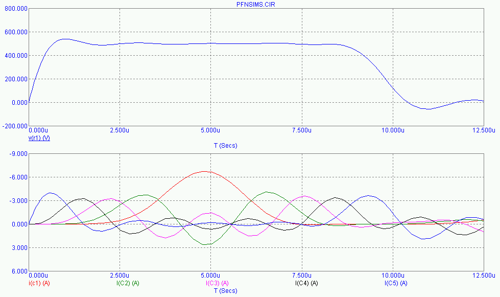
The circuit schematic and waveforms below show the individual capacitor currents and voltages for the 5 section Rayleigh Line Pulse Forming Network. For our example simulation, we use the same component values and initial conditions as above.
The results of the circuit model are shown below. V(R1) is the voltage across the load. The individual capacitor currents, I(C1) - I(C5), are graphed in the second, lower plot.
The waveform traces below again show the output pulse on the top half of the display and detail the individual capacitor voltages, V(C1) - V(C5), in the second, lower plot.
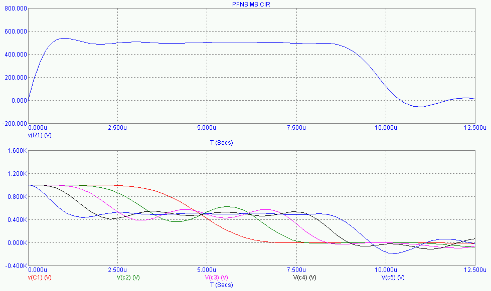
As one can see, the Pulse Forming Network section capacitors discharge sequentially, beginning with the capacitor closest to the load and finally working all the way back to the first capacitor.
The calculator below can be used to determine the proper section capacitance and inductance values for a Rayleigh Pulse Forming Network of a given configuration (based on pulsewidth, matching impedance, and number of desired sections). Credit for the initial Javascript code used in the calculator is given to Ray Allen who has a number of similar useful calculators on his website, Pulsed Power Portal.
Send consulting inquiries, comments, and suggestions to
nessengr@san.rr.com [HOME] [RESUME] [PUBLICATIONS] [NEWS] [LINKS] [CAPABILITIES] [TECHDATA]Ness Engineering, Inc.
P.O. Box 261501
San Diego, CA 92196
(858) 566-2372
(858) 240-2299 FAX
© Richard M. Ness and Ness Engineering, Inc. |
Website File Auto-Update Javascript courtesy of www.javafile.com Download the Script